Pmod connectors
The GECKO4-Education platform contains two double row Pmod connectors (PMOD1, PMOD2) and one “extended” single row Pmod connector (PMOD3) as shown in the figure below. The Pmod Interface specifications and a list of all available Pmods can be found here: *Digilen/PMOD*.
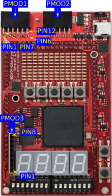
Pmod connectors on the GECKO4-Education-EPFL.
Warning
All I/O pins and clock pins of the Pmod connectors are 3.3V compliant. When using the I/O pin(s) as input(s), or when using the clock input(s), make sure that the voltage levels are between 0V and 3.3V, otherwise you may damage the FPGA!
Info
Make sure that the total current drawn from the 3.3V supply of the Pmod connectors does not exceed 250mA. Exceeding this limit may cause the board to malfunction or, in extreme cases, destroy it.
Double row Pmod connectors
The table below lists the double row Pmod connectors and their respective connections to the FPGA. An example tcl-script that can be used for the pin assignment is available here: pmod.tcl.
PMOD1
Pmod pin |
Function |
FPGA pin |
Pmod pin |
Function |
FPGA pin |
|---|---|---|---|---|---|
1 |
I/O 1 |
PIN_F2 |
7 |
I/O 7 |
PIN_F1 |
2 |
I/O 2 |
PIN_E3 |
8 |
I/O 8 |
PIN_E4 |
3 |
I/O 3 |
PIN_C2 |
9 |
I/O 9 |
PIN_C1 |
4 |
I/O 4 |
PIN_B2 |
10 |
I/O 10 |
PIN_B1 |
5 |
GND |
11 |
GND |
||
6 |
3V3 |
12 |
3V3 |
PMOD2
Pmod pin |
Function |
FPGA pin |
Pmod pin |
Function |
FPGA pin |
|---|---|---|---|---|---|
1 |
I/O 1 |
PIN_G5 |
7 |
I/O 7 |
PIN_H1 |
2 |
I/O 2 |
PIN_G4 |
8 |
I/O 8 |
PIN_J3 |
3 |
I/O 3 |
PIN_G3 |
9 |
I/O 9 |
PIN_J2 |
4 |
I/O 4 |
PIN_H2 |
10 |
I/O 10 |
PIN_J1 |
5 |
GND |
11 |
GND |
||
6 |
3V3 |
12 |
3V3 |
Single row Pmod connector
The table below lists the single row “extended” Pmod connector and the respective connections to the FPGA. An example tcl-script that can be used for the pin assignment is available here: pmod_ext.tcl. The Pmod “extended” connector has been extended with two additional pins that are directly connected to the clock inputs of the FPGA. This allows two external clock sources to be used to synchronise an external system with the FPGA.
PMOD3
Pmod pin |
Function |
FPGA pin |
|---|---|---|
1 |
I/O 1 |
PIN_AA16 |
2 |
I/O 2 |
PIN_AB16 |
3 |
I/O 3 |
PIN_AA15 |
4 |
I/O 4 |
PIN_AB15 |
5 |
GND |
|
6 |
3V3 |
|
7 |
CLK 1 |
PIN_AA12 |
8 |
CLK 2 |
PIN_AB12 |
Warning
When using a standard single row Pmod module, make sure that the PCB of this module faces to the left of the GECKO4-Education platform (the PCB position is marked by a thick white line to the left of PMOD3) and that the two clock pins are not connected to any of the pins of the Pmod module.