Arduino compatible connector
The GECKO4-Education platform has an Arduino Mega compatible connector architecture on it’s bottom side as shown in the figure below.
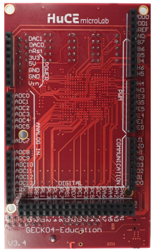
Arduino compatible connector on the bottom side of the GECKO4-Education platform.
Warning
All digital signals on the Arduino connectors are 3.3V compliant. Never connect a digital output with higher voltage levels (e.g. 5V) to these pins, as this will destroy the FPGA!
Info
For all analog pins please refer to the datasheets of the ADC and DAC that can be found here: ADC/DAC.
Power and reference voltage
The GECKO4-Education can be powered by connecting an external power supply to the Vin pin on the POWER connector. The voltage that can be applied to the Vin pin must be between 6.5V and 20V. Note that the higher the voltage, the warmer the LDO (Low Drop Out Regulator) on the top of the GECKO4-Education. If an external voltage is applied to the Vin pin, the GECKO4-Education will automatically switch to this power supply and decouple the USB power.
The GECKO4-Education provides two voltages at the power connector, namely 3.3V and 5V. The maximum total current drawn from these supplies is listed in the table below. Note that you must also take into account the current drawn by any Pmod modules connected!
Supply voltage |
USB-powered |
Vin-powered |
|---|---|---|
3.3V |
< 250mA |
< 500mA |
5V |
< 160mA |
< 400mA |
Finally, the GECKO4-Education provides pin AREF for use as an analog reference voltage. More information about this pin can be found here.
Analog connections
The GECKO4-Education platform provides 14 analog inputs (ADC0…ADC13) for the ADC on the ANALOG IN connectors. Pin ADC0 is connected to the input of the ADC with address 0, ADC1 to the input of the ADC with address 1, and so on.
The GECKO4-Education platform also provides two analog outputs (DAC0 and DAC1) for the DAC on the NC pins of the Arduino POWER connector. DAC0 is connected to channel 0 of the DAC and DAC1 is connected to channel 1.
Info
For information about the ADC and DAC, please refer to the ADC/DAC subsection of this documentation.
Digital connections
The GECKO4-Education board provides a variety of digital connections. The following sections list them all, including the FPGA connections.
PWM
The PWM connector contains 14 digital I/O pins. The table below lists these pins and their respective connections to the FPGA. An example tcl-script for connecting the PWM pins to the FPGA is available here: pwm.tcl.
Name |
Arduino pin |
FGPA pin |
|---|---|---|
PE0 |
0 |
PIN_M16 |
PE1 |
1 |
PIN_M19 |
PE4 |
2 |
PIN_N16 |
PE5 |
3 |
PIN_N17 |
PG5 |
4 |
PIN_P20 |
PE3 |
5 |
PIN_R22 |
PH3 |
6 |
PIN_R21 |
Name |
Arduino pin |
FGPA pin |
|---|---|---|
PH4 |
7 |
PIN_R20 |
PH5 |
8 |
PIN_U22 |
PH6 |
9 |
PIN_W22 |
PB4 |
10 |
PIN_W21 |
PB5 |
11 |
PIN_W20 |
PB6 |
12 |
PIN_V21 |
PB7 |
13 |
PIN_V22 |
Communication
The COMMUNICATION connector contains eight digital I/O pins. The table below lists these pins and their respective connections to the FPGA. An example tcl-script for connecting the COMMUNICATION pins to the FPGA is available here: communication.tcl.
Name |
Arduino pin |
FGPA pin |
|---|---|---|
PJ1 |
14 |
PIN_P21 |
PJ0 |
15 |
PIN_P22 |
PH1 |
16 |
PIN_N20 |
PH0 |
17 |
PIN_N21 |
PD3 |
18 |
PIN_N22 |
PD2 |
19 |
PIN_M20 |
PD1 |
20 |
PIN_M21 |
PD0 |
21 |
PIN_M22 |
Digital
The DIGITAL connector contains two 5V and two GND pins as well as 32 digital pins. The table below lists these pins and their respective connections to the FPGA. An example tcl-script for connecting the DIGITAL pins to the FPGA is available digital.tcl.
Name |
Arduino pin |
FGPA pin |
|---|---|---|
PA0 |
22 |
PIN_P16 |
PA1 |
23 |
PIN_T17 |
PA2 |
24 |
PIN_P17 |
PA3 |
25 |
PIN_T18 |
PA4 |
26 |
PIN_R18 |
PA5 |
27 |
PIN_T16 |
PA6 |
28 |
PIN_R19 |
PA7 |
29 |
PIN_T15 |
PC7 |
30 |
PIN_N15 |
PC6 |
31 |
PIN_R17 |
PC5 |
32 |
PIN_N14 |
PC4 |
33 |
PIN_R16 |
PC3 |
34 |
PIN_P15 |
PC2 |
35 |
PIN_R15 |
PC1 |
36 |
PIN_P14 |
PC0 |
37 |
PIN_R14 |
Name |
Arduino pin |
FGPA pin |
|---|---|---|
PD7 |
38 |
PIN_U19 |
PG2 |
39 |
PIN_U15 |
PG1 |
40 |
PIN_V16 |
PG0 |
41 |
PIN_V15 |
PL7 |
42 |
PIN_W19 |
PL6 |
43 |
PIN_W17 |
PL5 |
44 |
PIN_Y17 |
PL4 |
45 |
PIN_W15 |
PL3 |
46 |
PIN_AA19 |
PL2 |
47 |
PIN_AB19 |
PL1 |
48 |
PIN_AA18 |
PL0 |
49 |
PIN_AB18 |
PB3 |
50 |
PIN_AA17 |
PB2 |
51 |
PIN_AB17 |
PB1 |
52 |
PIN_U12 |
PB0 |
53 |
PIN_T12 |
Extra
Finally, the GECKO4-education platform provides five additional digital pins. The following table lists these pins and their respective connections to the FPGA. An example tcl-script for connecting these pins to the FPGA is available here.
Name |
FPGA pin |
|---|---|
PDD0 |
PIN_U20 |
PDD1 |
PIN_U12 |
CRX |
PIN_AA14 |
CTX |
PIN_AB14 |
nRst |
PIN_Y13 |