Buttons & DIP switches
The GECKO4-Education platform has seven push-buttons and two 8-position DIP switches as shown in the figure below.
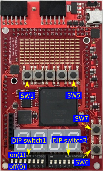
Buttons and DIP switches on the GECKO4-Education-EPFL.
Info
All buttons and DIP switches are active low, i.e. when pressed or in the “ON” position they provide a logic level of 0, and when not pressed or in the “OFF” position they provide a logic level of 1.
Each of these switches is connected to an individual FPGA-pin. Furthermore, all switches do not include an anti-dender circuit and the seven buttons are connected to clock-inputs of the FPGA.
Buttons
The table below lists the buttons and their respective connections to the FPGA. An example tcl-script that can be used for the pin assignment is available here: switches.tcl.
Button |
FPGA pin |
|---|---|
SW1 |
PIN_B11 |
SW2 |
PIN_A11 |
SW3 |
PIN_B12 |
SW4 |
PIN_A12 |
SW5 |
PIN_G22 |
SW6 |
PIN_AA11 |
SW7 |
PIN_AB11 |
Info
All seven buttons are connected to clock-inputs of the FPGA and can therefore be used as clock sources.
DIP switches
The table below lists the two 8-position DIP switches and their respective connections to the FPGA. An example tcl-script that can be used for the pin assignment is available here: dip_switches.tcl.
Switch |
FGPA pin |
|---|---|
1 |
PIN_V11 |
2 |
PIN_V10 |
3 |
PIN_AB10 |
4 |
PIN_AA10 |
5 |
PIN_AB9 |
6 |
PIN_AA9 |
7 |
PIN_AB8 |
8 |
PIN_AA8 |
Switch |
FGPA pin |
|---|---|
1 |
PIN_Y8 |
2 |
PIN_AB7 |
3 |
PIN_AA7 |
4 |
PIN_Y7 |
5 |
PIN_Y6 |
6 |
PIN_AB5 |
7 |
PIN_AA5 |
8 |
PIN_AB4 |
Info
All DIP switches require a pull-up resistor to function correctly. The pull-up resistors can be enabled separately for each switch in the dip_switches.tcl.