Memory
The GECKO4-Education platform contains SDRAM and serial flash memory as shown in the figure below.
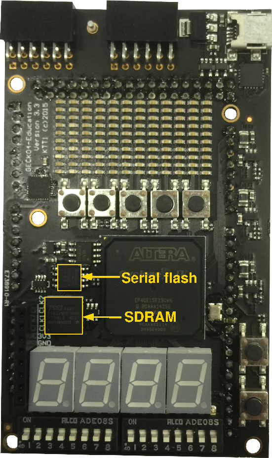
SDRAM and Flash on the GECKO4-Education platform.
SDRAM
The GECKO4-Education contains a 32MByte mobile synchronous DRAM (M-SDRAM). This SDRAM can be used with the QSYS external SDRAM memory controller. The tables below show the FPGA pins to which the SDRAM is connected. Here: sdram.tcl is an example tcl script that can be used for the pin assignment in Quartus.
Address bus
Address bit |
FPGA pin |
|---|---|
0 |
PIN_N5 |
1 |
PIN_N6 |
2 |
PIN_P4 |
3 |
PIN_P5 |
4 |
PIN_W6 |
5 |
PIN_V7 |
6 |
PIN_V6 |
Address bit |
FPGA pin |
|---|---|
7 |
PIN_V5 |
8 |
PIN_V1 |
9 |
PIN_V4 |
10 |
PIN_U2 |
11 |
PIN_U8 |
12 |
PIN_V2 |
Data bus
Data bit |
FPGA pin |
|---|---|
0 |
PIN_M1 |
1 |
PIN_M2 |
2 |
PIN_M3 |
3 |
PIN_N1 |
4 |
PIN_N2 |
5 |
PIN_P1 |
6 |
PIN_P2 |
7 |
PIN_P3 |
Data bit |
FPGA pin |
|---|---|
8 |
PIN_W1 |
9 |
PIN_W2 |
10 |
PIN_Y1 |
11 |
PIN_Y2 |
12 |
PIN_Y3 |
13 |
PIN_AA1 |
14 |
PIN_AB3 |
15 |
PIN_AA4 |
Control signals
Function |
Name |
FPGA pin |
|---|---|---|
Bank select low |
BA[0] |
PIN_M6 |
Bank select high |
BA[1] |
PIN_M7 |
Byte select low |
DQM[0] |
PIN_R1 |
Byte select high |
DQM[1] |
PIN_V3 |
Clock enable |
CKE |
PIN_U7 |
Clock |
CLK |
PIN_AA3 |
Column address select (active low) |
nCAS |
PIN_M5 |
Row address select (active low) |
nRAS |
PIN_M4 |
Chip select (active low) |
nCS |
PIN_U1 |
Write enable (active low) |
nWE |
PIN_R2 |
Flash
In addition to the FPGA configuration FLASH, the GECKO4-Education platform also contains an 8MByte serial FLASH memory. The tables below show the FPGA pins to which the Flash is connected. Here: flash.tcl is an example tcl script that can be used for the pin assignment in Quartus.
Function |
Name |
FGPA pin |
|---|---|---|
Chip select (active low) |
NCS |
PIN_U14 |
Hold (active low) or IO3 |
NHOLD_IO3 |
PIN_U13 |
Serial clock |
SCK |
PIN_V13 |
Serial in or IO0 |
SI_IO0 |
PIN_W13 |
Serial out or IO1 |
SO_IO1 |
PIN_V14 |
Write protect (active low) or IO2 |
NWP_IO2 |
PIN_W14 |