IP-Architecture
Overview
To test the functionality of all hardware components on the GECKO-visual board the following IP-architecture was realized:

The IP-architecture is local to the GECKO-visual FPGA and has no link to the GECKO-main. A continuous stream of frames is taken from the camera and buffered into the SDRAM. The buffered data is then read out and displayed by the LCD. Main element of the design is the Xilinx multiport memory controller (mpmc) which controls the read and write accesses from and to the SDRAM. All components (IP-Cores) are discussed in detail in the following sections.
Data Flow
In this section the flow of the pixel data from the camera to the display is explained.
Write Data
The camera has a bayer pattern image filter which means each pixel corresponds to one single color. Because of the eyes sensitivity to green, the green color is dominant and delivered twice.
The selected camera resolution is 1.3 MP which corresponds to 1280×960. Each pixel has a data width of 10-bit. The following picture shows the scan direction and order of pixel:
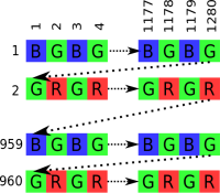
To reconstruct a full color image (RGB) a so called demosaicing is performed. With the color information of two lines one single line in RGB is generated.
First one odd line and one even line from the camera are buffered into two separate line fifo's (8 msb out of 10). The input data width of the line fifo is 8-bit, the output data width is 16 bit. This approach results in less read cycles.
From the data outputs of odd and even line fifo one single RGB pixel is formed. The red and blue values are copied directly, the green value is generated by the average of both green values. The most significant byte of the pixel data remains empty. The data is then buffered into a 32-bit fifo. From there the data is read and written into the SDRAM.
![]()
The described demosaic process results in an image with half the size of the input data. The new image size is 640×480 which is still enough for the display resolutoin (320×480).
Read Data
The image which is located in the SDRAM can now be read out line by line. Due to the smaller size of the display only a sub section of the size of 320×480 is taken. The pixel data in the memory has a bit width of 8 per color. The display supports only 18-bit RGB and so only the 6 most significant bit of each color are sent to the display.
![]()
Tools
Xilinx XPS
The IP-Architecture was created with Xilinx Platform Studio 13.1 (XPS). XPS allows the use of Xilinx proprietary IP-cores as well as user defined IP-cores (PCores).
Type the following in the linux terminal to start XPS 13.1:
ssh -X hercules
xilinx_version_selection 13.1
xps
MHS File
XPS is a graphical tool to connect and configure several IP-Cores and create an IP-architecture. All system information is stored in the system.mhs configuration file. In a first section of the mhs file the ports are defined. Afterwards all used IP-Cores with their parameters are listed.
UCF File
In the UCF file the defined ports are assigned(mapped) to the physical IO pins of the FPGA. Also all constraints and attributes (e.g. timing constraints) are placed here. More details concerning Xilinx constraints you will find in the Xilinx Constraints Guide.
PCores
User defined IP-Cores (PCores) are located inside the pcores directory in the XPS project folder. The file structure for an example IP-Core named pcore_v1_00a is as follows:
- XPS Project Folder
- pcores
- pcore_v1_00_a
- data
- .bbd
- .mpd
- .pao
- devl
- -
- hdl
- vhdl
- .vhd files
- netlist
- .ngc files
.mpd File (Microprocessor Peripheral Description)
Provides default parameters and options for the PCore device in XPS:
- Peripheral Options
- Bus Interfaces and Parameters
- Signals and Ports accessible from XPS
.bbd File (Black-Box Definition)
Manages the file locations of hardware netlists for the black box sections of the PCore.
.pao File (Peripheral Analysis Order)
Contains the list of HDL files that are needed for synthesis and defines the analyze order for compilation.
vhdl Folder
The vhdl Folder contains all .vhd files.
netlist Folder
The netlist Folder contains all .ngc files (Black Box Files).
The XPS design is located in the following directory:

/mnt/data/fbe/microlab/projekte/intern/GECKO/GECKO_AddOn/GECKO_visual/version_1/03_Firmware/XPS
Xilinx ISE
Xilinx ISE was used for netlist generation of specific parts of the IP-Architecture (e.g. fifo's and rom's). The CORE Generator is part of ISE and allows the generation of parameterizable cores optimized for Xilinx FPGA's. The output files of the CORE Generator are located in the ipcore directory of the ISE project folder:
- ISE Project Folder
- ipcore_dir
- .vhd
- .ngc
.vhd Files
The .vhd files contain the definition and parameters of the associated core. These files are used for simulation purposes.
.ngc Files
The netlist files of the associated core. If used in a PCore within XPS, these files have to be copied into the netlist directory of the PCore.
The ISE Project is located in the following directory:
/mnt/data/fbe/microlab/projekte/intern/GECKO/GECKO_AddOn/GECKO_visual/version_1/03_Firmware/ISE
Xilinx SDK
The Xilinx SDK (Software Development Kit) is used to develop software applications for the Xilinx Microblaze soft-core processor. In the example design no Microblaze is present and therefore the Xilinx SDK is not used.
IP-Cores
Xilinx MPMC
MPMC is a fully parameterizable multiport memory controller that supports SDRAM. MPMC provides access to memory for one to eight ports, where each port can be chosen from a set of interface types.
In our IP-architecture, only two ports are used (one for the Camera-IP and one for the Display-IP). The interface type used is the Native Port Interface(NPI) which offers a simple way to directly access the memory through the MPMC. The NPI provides address, data, and control signals to enable read and write requests for memory.
Different arbitration algorithms can be selected in the MPMC configuration. In this application, the fixed arbitration is used. In this mode the priority is fixed so that the lowest Port has the highest priority.
The MPMC is configured in the system.mhs.
Find all details in the mpmc datasheet.
ar24912.zip provides an example of an NPI-PCore which performs read and write cycles.
Camera NPI
The purpose of the Camera NPI IP-Core is to write the camera data continuously into the SDRAM. During this operation, camera data is converted from bayer-pattern structure into RGB data structure. Read more about this process in the Data Flow chapter.
The following figure shows a detailed the structure of the Camera NPI:
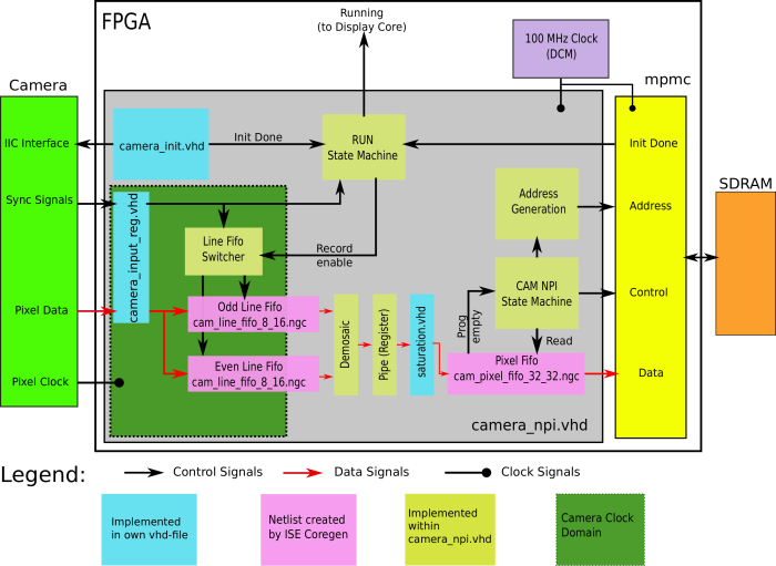
camera_init.vhd
Consists of a simple state machine which initializes the camera module. The camera is put into 1.3 MP mode and “flip and mirror” is enabled. The “init done” line signals the end of the initialisation process.
RUN State Machine
Combines the “init done” signals from the camera init process and the mpmc. After receiving both signals, the RUN State Machine waits until a new frame begins(rising edge on vsync) and then starts the recording process.
camera_input_reg.vhd
All camera signals are registered before further processing. These registers are placed directly in the IOB's of the FPGA device and clocked by the external camera clock.
Line Fifo Switcher
The odd and even line are buffered into two independent fifos. The Line Fifo Switcher uses the synchronisation signals (vsync and hsync) to choose the correct fifo for incoming pixel data.
cam_line_fifo_8_16.ngc
Fifo to buffer incoming camera data. Camera data is written on the rising edge of the camera clock. The fifo allows different read and write clocks and serves also as clock domain crossing mechanism. The input data width is 8 bit, the output data width is 16 bit. Two instances of this fifo are used (odd and even line).
Demosaic
The demosaic stage combines 2 pixels from the odd line fifo with 2 pixels from the even line fifo and creates a single RGB pixel (see also Chapter Data Flow).
Pipe
A simple register serves as pipeline between the demosaic and saturation stage and allows a higher processing speed.
saturation.vhd
In this processing step the most dominant color is amplified which leads to more deep color in the final image on the display. This algorithm is a very simple approach and has to be approved in a further design.
cam_pixel_fifo_32_32.ngc
In this fifo the processed image data is stored temporarily before data is written into the SDRAM. The fifo has a programmable empty signal which shows when the data of 8 pixel are ready to read.
CAM NPI State Machine
This state machine controls the write process to the SDRAM. The write process signaling is shown in the following image:

The selected write mode is “8-word cacheline transfer”. 1 word corresponds to 32-bit which is equal to 1 pixel. If 8 pixel from the pixel fifo are ready to read(prog empty), the data is read out and written into the fifo of the memory controller. After this an address request is done. If the address request is acknowledged, the address is incremented and the process starts again.
After the data acknowledge the mpmc core writes the data by itself into the SDRAM.
Address Generation
The address generation circuit is triggered by the CAM NPI State Machine. The Address is incremented in steps of 32. 32 equals to 8 words of 4 bytes(8 pixels). If a whole image is written (640x480x4byte), the address wraps around and starts again with 0x00000000h.
Display NPI
The display NPI IP-core reads the camera data from the SDRAM and brings the data to the display. The following image shows the architecture of this IP-core:

diplay_init.vhd
A state machine which initializes the display via the SPI interface. The initialization data is taken from the initialisation ROM.
DISP_INIT_ROM.ngc
Netlist of the initialisation ROM.
display_logic.vhd
The pixel data is transferred by the RGB data interface. The display_logig.vhd block reads the pixel fifo and generates the pixel clock as well as the synchronisation signals:

Display NPI State Machine
The display NPI State Machine controls the read cycles from the SDRAM. The signaling of the read process is shown in the following image:

After receiving the init done and the running signal the state machine starts to generate read requests. If a read request is accepted the data is taken out and written into the pixel fifo. The data is read in 8-word bursts. After each read cycle the address generation is activated.
Address Generation
The address generation circuit is triggered by the Display NPI State Machine. The Address is incremented in steps of 32. The address generation selects a section of 320×480 pixel in the memory.