Table of Contents
Hardware
In this section all hardware components are introduced. The block diagram gives an overview of the interconnection of components. Main part is the Spartan 3an FPGA which serves as central unit.
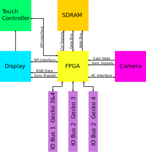
Find more information about the functional interaction of the components in the section ip-architecture.
Hardware Components
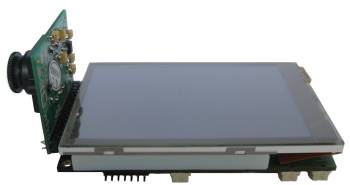
Display
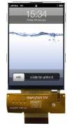
The display is a 480×320 Pixel transmissive LCD which fulfills the size requirements of the GECKO system standard. For backlighting an external backlight driver is needed (TPS61160A). Two interfaces are provided: SPI for configuration and parallel RGB for Display data.
- Module Name: SDT033TFT Datasheet
- Driver IC: D51E5TA7601 Datasheet
- Mode: Transmissive LCD
- Colors: 256k
- Data Interface: 18 Bit RGB
- Control Interface: SPI
- Size: 3.5 Inch
- Resolution: 480 x 320 Pixels
- Touch Screen: 4 Wire Resistive
- Used Backlightdriver IC: TPS61160A Datasheet
Touch Controller
The display includes a resistive touch screen which can be used with an external touch screen controller. The popular Microchip AR1020 is used which drives the touch screen lines and converts the analog signal into digital position data.
- Microchip AR1020 Datasheet
- Type: Analog Resistive 4-, 5- or 8-Wire
- Interface: SPI / IIC
- ADC: Internal 10 Bit
Camera Module
The camera module houses a 5 MP CMOS image sensor from omnivision. The image data is provided by a 10 bit RGB Raw Data interface. The color filters are in Bayer Pattern. An IIC interface is used for configuration purposes.

- Module: COMedia OV5620 Datasheet
- Image Sensor: Omnivision OV5620 Datasheet
- Resolution: 5MP (2592×1944)
- Data Interface: 10 bit RGB Raw Data
- Control Interface: IIC
The sensor provides different resolutions and framerates:
| Format | H-Size | V-Size | Framerate(fps) |
|---|---|---|---|
| 5 Mpixel | 2592 | 1944 | 7.5 |
| 1.3 Mpixel | 1280 | 960 | 30 |
| D1MD | 864 | 600 | 60 |
| QFMD | 1280 | 480 | 60 |
| HF | 1280 | 240 | 120 |
It can be seen that a continuous video stream to the display(resolution 320×480) is possible.
SDRAM
The SDRAM serves as video frame buffer. The used memory has a capacity of 128 Mbit and allows the storage of around 50 frames (framesize:320x480x18bit). The memory is controlled by the Xilinx Multiport Memory Controller(mpmc) IP-Core.
- ESMT M52D128168A2P
- Memory Type: SDRAM
- Capacity: 128 Mbit
- Speed: 133 MHz
- Organisation: 2M x 16bit x 4banks
- Package: TSOPII
FPGA
The FPGA serves as central unit which interconnects and controls all HW-components. With FPGA's of the Spartan 3an series no external configuration flash is needed. The FPGA includes 4Mbit internal flash which allows the storage of the configuration data (bit-file).
| Device | System Gates | Distr. RAM | Block RAM | DCMs | User IO | Flash |
|---|---|---|---|---|---|---|
| XC3S200AN | 200k | 28 kbit | 288 kbit | 4 | 192 | 4Mbit |
PCB Design
PCB design was done by altium designer ECAD. The design files are located in the following directory:
/mnt/data/fbe/microlab/projekte/intern/GECKO/GECKO_AddOn/GECKO-visual/version_1/02_PCB
Schematic
Powering
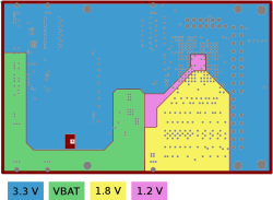
The following table shows the supply voltage of the main components:
| Component | 3.3 V | 1.8 V | 1.2 V | 18 V |
|---|---|---|---|---|
| Display | ✔ | |||
| Display Backlight | ✔ | |||
| Touch Controller | ✔ | |||
| Camera | ✔ | |||
| SDRAM | ✔ | |||
| FPGA | ✔ | ✔ | ✔ |
+3V3 of system bus 1 is not used.
The different supply voltages are provided by split planes located on the inner power plane of the PCB:
PCB Layout
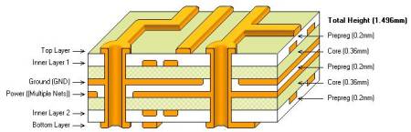
The image shows the PCB Stackup. The PCB consists of 4 signal layers and 2 power planes (located in the middle).
Layout FPGA
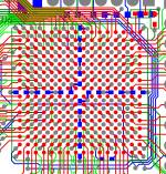
The FPGA comes in a FT256 BGA with 1mm pitch. To route the I/O's vias are placed between each pin:
Layout SDRAM
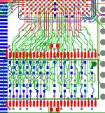
Due to the high speed of SDRAM signals all lines to the memory are length matched:
Final Result