Project details
| Name: | GECKO3EDU | |
|---|---|---|
| Maintainer | orphaned | |
| Revision: | unknown | |
| Development status: | stable | |
| Compatibility: | GECKO3 | |
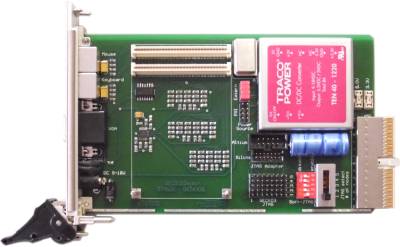
GECKO3 staddle
This platform is designed to operate a stack of several gecko3 modules and to give them computer-like interfaces.
Features
- Euro card 3U form factor with frontpanel to assemble in modular chassis like PXI
- board powering via the PXI backplane or a standard DC adapter with a voltage range of 9V up to 18V
- current supply of up to 8A with external power (sufficient for 4-5 GECKO3main modules)
- two PS2 ports for mouse and keyboard
- a VGA port for monitor outputs with 16 bit color resolution and 1280×1024 display resolution
- supports Altium Designer's Nexus-Soft-JTAG and Xilinx JTAG
- distributes the JTAG chain to the modules of the stack
- global clock to synchronize the GECKO3STACK
JTAG
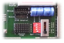
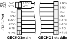 The platform makes it possible to configure and debug the GECKO3main modules with Xilinx tools and with Altium Designer. For this reason, a 14-pin (
Xilinx) and a 10-pin (Altium) JTAG adapter port is installed on the board. While the GECKO3main module is already equipped to use the Xilinx JTAG interface, the additional Soft-JTAG feature of Altium Designer requires four additional signals. The 6-pole connector of the JTAG GECKO3main modules is used for the Hard-JTAG chain (identical to Xilinx), and the Soft-TDI and Soft-TDO are sent on the pins, which are originally designed for the RS-232 connection. The two broadcast signals, Soft-TMS and Soft-TCK, are distributed to the modules through the system bus.
For the JTAG connection to the GECKO3main modules there are five eight pin headers provided on the board, labeled with GECKO3 JTAG and numbered. The no.1 pin is marked to avoid incorrect connection. A slide switch can bridge unconnected JTAG ports and enables the flexible use of up to five GECKO3main modules. The ports have to be occupied successively. The marking of the switch is JTAG select # of nodes. A DIP switch is installed to selectively enable the use of the Altium Designer soft-JTAG chain. The switch is labeled with Soft JTAG and its switch positions are marked with enable or disable.
For designs with Altium soft-JTAG devices the use of this adapted constraint file is required (it includes the mappings of the soft-JTAG signals to both the original RS232-header, and to GPIO-bus pins for distribution throughout the stack).
 gecko3_nexus.zip
PS/2
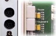
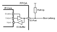 There are two PS/2 ports applied to the front panel for user input via keyboard and mouse. The signals are passed through the system bus to the GECKO3main modules. Since both, the input device and the FPGA can drive the line, a short circuit by different signal levels must be prevented. This can be realized using the tri-state outputs of the FPGA, but has to be taken care of by the PS/2 component within the FPGA design. A “zero” is given active to the output, but instead of an active “one”, the output is set high impedance (disable). The high level of the line is achieved by the external pull-up resistor to 5 V.
VGA
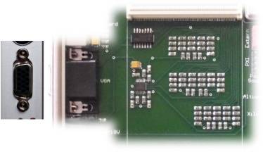
On the front panel of the card is also a VGA connector for the monitor output. The maximum depth is 16 bit (65,536 colors). In this “High Color” Graphics mode red and blue, each are coded with 5 bits and green stand for even 6 bits. If you use a display controller with less color resolution, you have to allocate the color signals from the most to the least significant bit. The remaining lines of the platform should assigned each to the least significant color bit of the controller IP core.
After the digital signals were transmitted to the platform, the color channels must be converted into analog signals (0 - 0.7V). We apply an R-2R network, as with the use of simple SMD resistors, high color resolution can be generated. Using an op amp the output of the network is discoupled from the load resistance of the monitor. To generate an image on the monitor to the VSYNC and HSYNC signals. These digital synchronization signals can be operated with a level of 3.3 volts and require no further processing. However, they should also be decoupled to protect the FPGA outputs.
Power Source
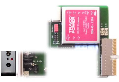 For power supply a DC/DC converter TEN 40-1220 by Traco Electronic is mounted on the platform. From an input voltage of 9-18 V it produces two output voltages of 3.3 V and 5 V. With the maximum output power of 40 W up to 5 GECKO3main modules can be operated. A external 12 volt power supply can be connected via a “Power Jack Connector 2.1 mm” at the front panel. Using four jumpers select between external power or PXI. For the PXI option the power is provided via the CompactPCI connector. The two voltages are each loaded with a maximum of 2 A (protected), so that on a staddle only one GECKO3main module can be operated inside a slot of a PXI rack.
System Bus Pin Assignment
For a fast communication between the modules a wide bus connection is needed. On this account, the GECKO3 staddle doesn't use the IO2 bus and so its 116 pins can completely be used for the GECKO3STACK intermodule communication protocol. An oscillator on the EXTCLK1 line enables the implementation of synchronous bus protocols. It is placed in a socket and can be substituted to vary the bus clocks.
On the EXTCLK0 pin is the SOFT_JTAG_TCK signal, because this has to be connected to a clock input of the FPGA. The SOFT_JTAG_TMS signal is on the adjacent GPIO1_2 pin. The other Soft JTAG signals are connected to the GECKO3main modules directly.
Due to the use of continuous areas for equal types of signals, the 18 digital lines to the VGA port are also located in the first section of the IO1 bus. The four signals of the PS2 interfaces are transmitted on lines on the higher connector section.
| Signal Name | Pin (IO1-Bus) | System Bus Pin Name |
|---|---|---|
| Soft JTAG Chain | ||
| SOFT_JTAG_TCK | 7 | EXTCLK0 |
| SOFT_JTAG_TMS | 11 | GPIO1_2 |
| VGA Interface | ||
| RED[4..0] | 27, 25, 23, 21, 19 | GPIO1_18, GPIO1_16, GPIO1_14, GPIO1_12, GPIO1_10 |
| GREEN[5..0] | 13, 15, 17, 14, 16, 18 | GPIO1_4, GPIO1_6, GPIO1_8, GPIO1_3, GPIO1_5, GPIO1_7 |
| BLUE[4..0] | 20, 22, 24, 26, 28 | GPIO1_9, GPIO1_11, GPIO1_13, GPIO1_15, GPIO1_17 |
| VSYNC, HSYNC | 4, 6 | GPIO1_0, GPIO1_1 |
| PS2 Interface | ||
| PS2M_DATA, PS2M_CLK | 85, 87 | GPIO1_20, GPIO1_22 |
| PS2K_DATA, PS2K_CLK | 86, 88 | GPIO1_23, GPIO1_21 |
Documents
Schematic:gecko3_staddle_schem.pdf
PCB design:gecko3_staddle_pcb.pdf

