Pinout
UCF File: gecko_visual.ucf
GECKO system bus 1 (IO-Bus 1)
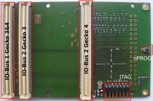
The mechanical position of the system bus 1 connector on GECKO3main and GECKO4main is similar. Therefor only 1 connector is needed.
| Pin | Name | Pin on Gecko Visual FPGA | Description |
|---|---|---|---|
| 1 | GND | - | System GND |
| 2 | GND | - | System GND |
| 3 | nRESET | P7 | Global Reset Pin |
| 5 | GND | - | System GND |
| 7 | EXTCLK0 | P8 | External Clock In0 |
| 8 | GND | - | System GND |
| 9 | GND | - | System GND |
| 10 | EXTCLK1 | P9 | External Clock In1 |
| 12 | GND | - | System GND |
| 29 | GND | - | System GND |
| 30 | GND | - | System GND |
| 33 | GND | - | System GND |
| 34 | GND | - | System GND |
| 35 | VBAT | - | Battery Power |
| 36 | VBAT | - | Battery Power |
| 37 | VBAT | - | Battery Power |
| 38 | VBAT | - | Battery Power |
| 39 | VBAT | - | Battery Power |
| 40 | VBAT | - | Battery Power |
| 41 | GND | - | System GND |
| 42 | GND | - | System GND |
| 43 | GND | - | System GND |
| 45 | GND | - | System GND |
| 46 | GND | - | System GND |
| 53 | GND | - | System GND |
| 54 | GND | - | System GND |
| 56 | GND | - | System GND |
| 59 | GND | - | System GND |
| 60 | GND | - | System GND |
| 81 | SDA | N7 | IIC Bus Data Line |
| 83 | SCL | P6 | IIC Bus Clock Line |
| 89 | GND | - | System GND |
| 90 | GND | - | System GND |
| 119 | GND | - | System GND |
| 120 | GND | - | System GND |
Unlisted pins are unused
GECKO system bus 2 (IO-Bus 2)
The mechanical position of the system bus 2 connector on GECKO3main and GECKO4main is not identical. To make the GECKOvisual compatible with both versions of GECKO-main, two different connectors are used (refer to image on top). The assignment of the pins on both connectors is similar.
| Pin | Name | Pin on Gecko Visual FPGA | Description |
|---|---|---|---|
| 1 | GND | - | System GND |
| 2 | GND | - | System GND |
| 5 | GPIO2_2 | R3 | Image Data Downstream |
| 6 | GPIO2_3 | T2 | Image Data Downstream |
| 7 | GPIO2_4 | T4 | Image Data Downstream |
| 8 | GPIO2_5 | R5 | Image Data Downstream |
| 9 | GPIO2_6 | T6 | Image Data Downstream |
| 10 | GPIO2_7 | T5 | Image Data Downstream |
| 11 | GPIO2_8 | R7 | Image Data Downstream |
| 12 | GPIO2_9 | T7 | Image Data Downstream |
| 13 | GPIO2_10 | T9 | Image Data Downstream |
| 14 | GPIO2_11 | T8 | Image Data Downstream |
| 15 | GPIO2_12 | T10 | Image Data Downstream |
| 16 | GPIO2_13 | P10 | Image Data Downstream |
| 17 | GPIO2_14 | T11 | Image Data Upstream |
| 18 | GPIO2_15 | P11 | Image Data Upstream |
| 19 | GPIO2_16 | P12 | Image Data Upstream |
| 20 | GPIO2_17 | T13 | Image Data Upstream |
| 21 | GPIO2_18 | P13 | Image Data Upstream |
| 22 | GPIO2_19 | T14 | Image Data Upstream |
| 23 | GPIO2_20 | R9 | Image Data Upstream |
| 24 | GPIO2_21 | R11 | Image Data Upstream |
| 25 | GPIO2_22 | N11 | Image Data Upstream |
| 26 | GPIO2_23 | R14 | Image Data Upstream |
| 27 | GPIO2_24 | N12 | Image Data Upstream |
| 28 | GPIO2_25 | R13 | Image Data Upstream |
| 29 | DONE | T15 | FPGA Done Pin |
| 30 | nPROG | A2 | FPGA nPROG Pin |
| 119 | GND | - | System GND |
| 120 | GND | - | System GND |
Unlisted pins are unused
Define DONE and nPROG signals as input on the GECKO-main FPGA. Otherwise the function of the GECKO-visual will be affected.